Electronics & Probes by Materials Engineering

Materials
become
electronics.

Built on single-crystalline metal nanosheets and integrated fiber electronics, our DGIST research advances materials from atomic-scale discovery to energy-managing systems.

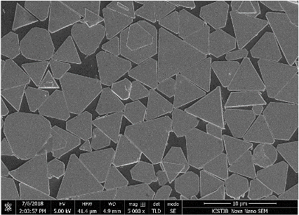
Scanning electron microscopy image of single-crystalline copper nanosheets
2D MaterialsDevicesIntegrated Systems
APPND / MATERIAL 01Single-crystalline
metal nanosheets
MaterialsInterfacesDevicesSystems

Our research question

How can dimensional engineering turn metals into active electronic systems?

APPND connects a proven foundation in 2D single-crystalline metals, interface-controlled devices, and chip-on-fiber integration with a new DGIST vision: atomically thin metallene, scalable manufacturing, emerging 1D electronics, and smart energy skins.

01

Build the matter

2D Metals
& Metallene

We control crystal growth, dimensionality, porosity, composition, and surface chemistry—from single-crystalline metal nanosheets toward sub-5 nm metallene and multifunctional materials platforms.
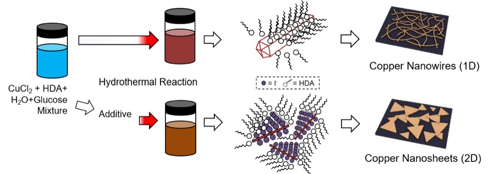
Copper nanosheet solution-synthesis process
Solution synthesis / Cu nanosheets
Scanning electron micrograph of densely packed copper nanosheets
Single-crystal growth
Layered copper nanosheet electromagnetic shielding film
Hierarchical assembly

From a nanosheet in solution to a macroscopic conducting network and multifunctional platform.

  • Single crystalsLarge-area Cu and Ag nanosheets with controlled facets and interfaces
  • Metallene frontierSub-5 nm 2D metals and electronically tunable metal–halide derivatives
  • Digital discoverySimulation, data, and AI-assisted synthesis for faster materials design
  • Architected filmsIsotropic, porous, ultrathin, and omni-directionally assembled structures
Foundation → frontierMetal nanosheets · Metallene · Architected films

Materials engineering applications

Application 01

Self-powered

Hierarchical porous metal nanosheet triboelectric generators and sensing platforms

Application 02

Thermal & EMI

Low-voltage Joule heating, radiative cooling, and electromagnetic shielding

Application 03

Energy interfaces

Active current collectors and multifunctional nanosheet films for energy systems

02

Program the function

Semiconductor &
Neuromorphic Devices

We engineer semiconductor materials, charge transport, contacts, and active interfaces to realize transistors, nonvolatile memories, and neuromorphic devices.

Semiconductor interfaces become logic, memory, and adaptive computing.
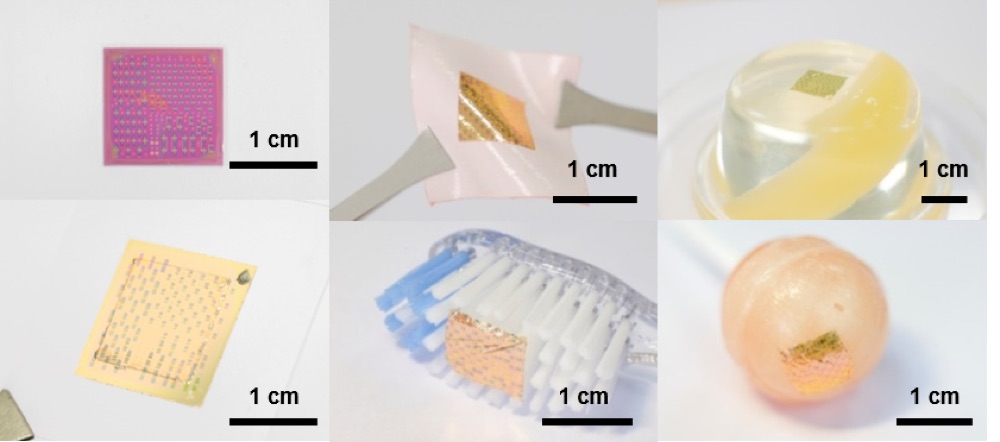
  • Semiconductor interfacesEnergy-level alignment, contacts, defects, and charge transport across active interfaces
  • Thin-film transistorsOxide and organic transistors with stable switching and precisely engineered threshold voltage
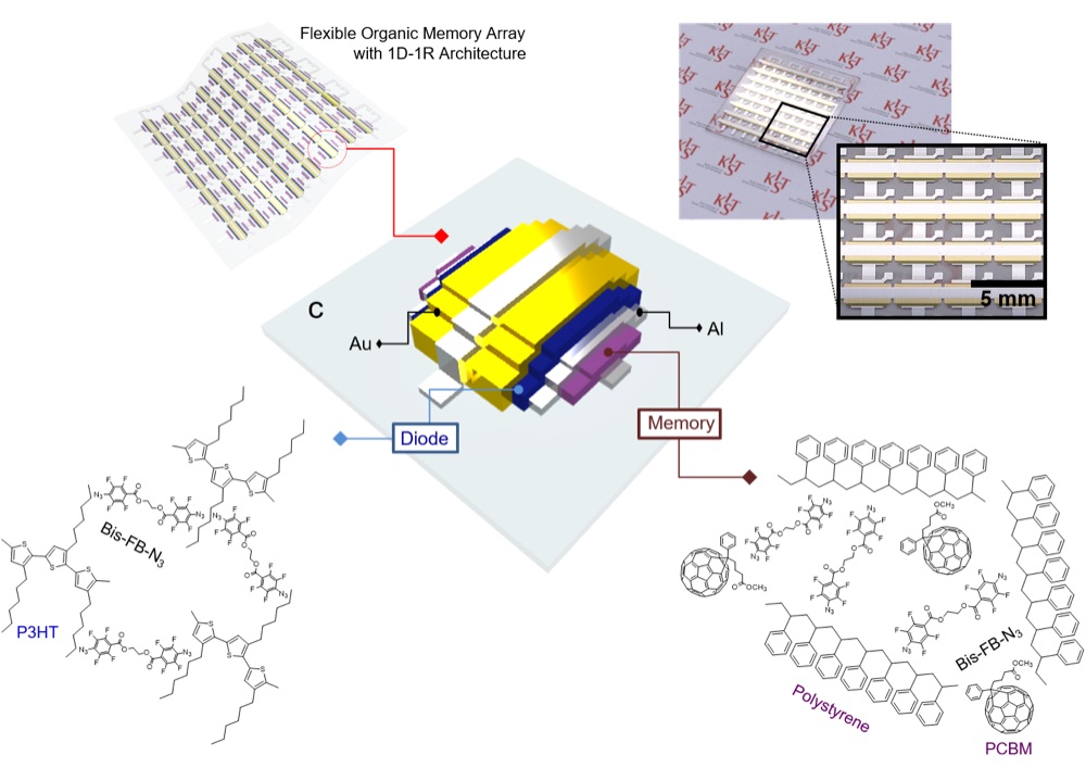
  • Nonvolatile memoriesFlexible memory devices based on charge trapping, ferroelectricity, and resistive switching
  • Neuromorphic devicesSynaptic transistors and memory elements for learning, adaptation, and in-memory computing
Interfaces → intelligenceTransistors · Memories · Neuromorphic devices
Ultrathin ferroelectric organic neuromorphic transistor
Neuromorphic transistor
Flexible and twistable organic memory device
Flexible memory
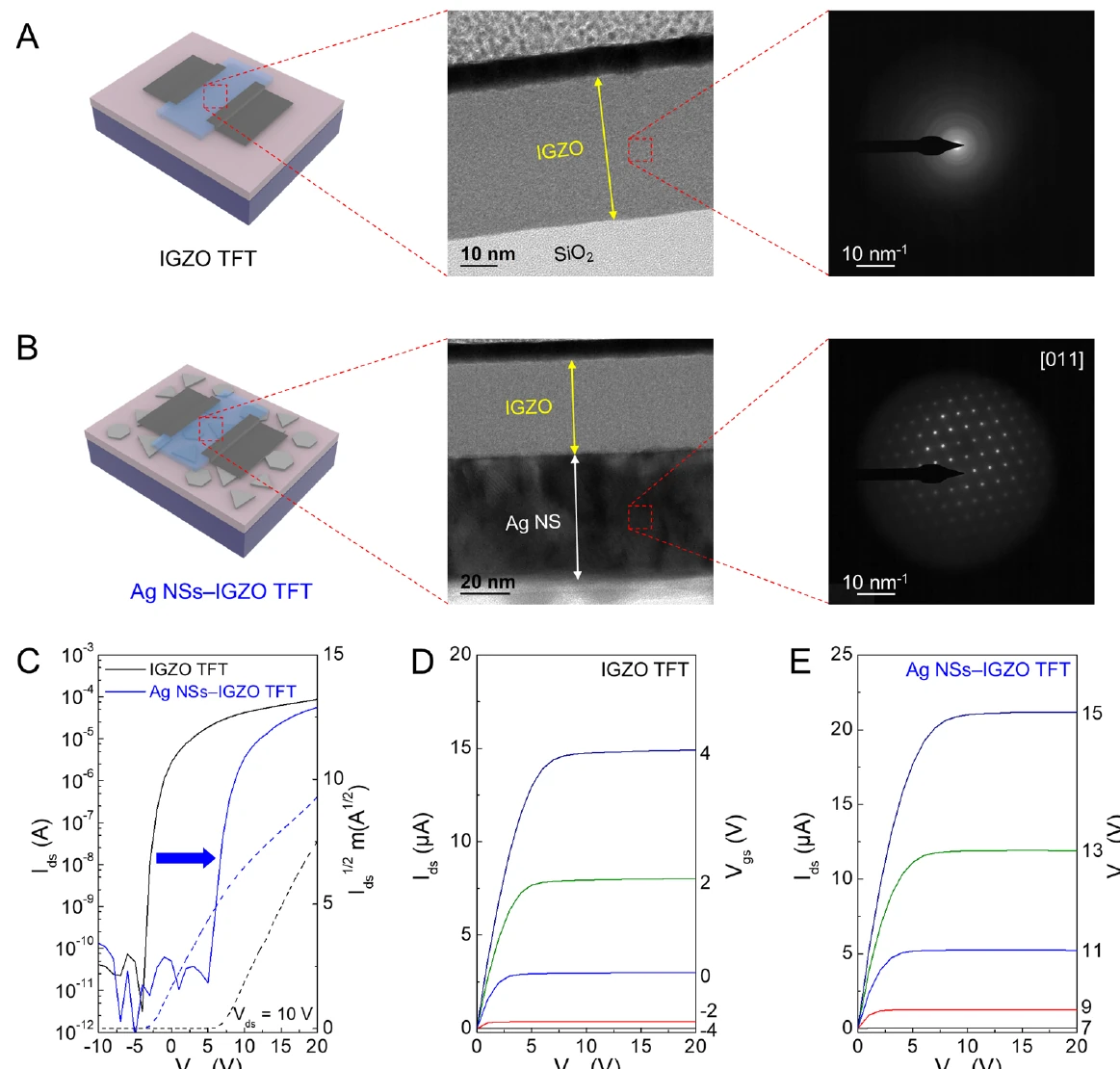
Silver nanosheet interface integrated with an oxide thin-film transistor
Oxide TFT interface
03

Move beyond the wafer

Emerging 1D
Electronics

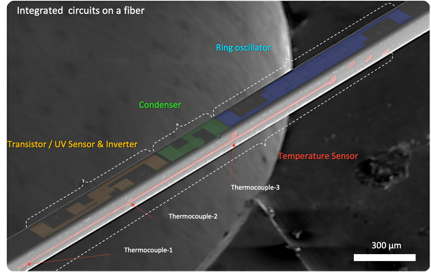
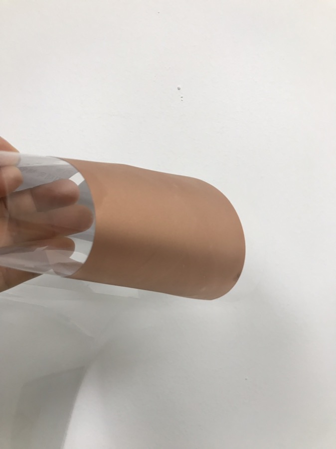
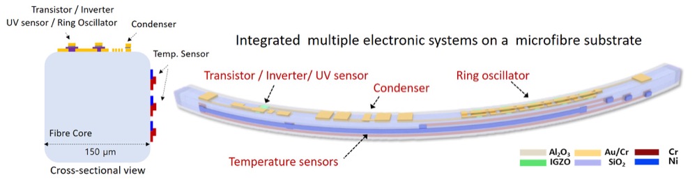
We build electronics along fibers and hollow one-dimensional architectures, using both exterior and interior surfaces for distributed computing, sensing, energy harvesting, and active regulation.
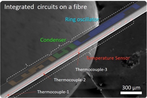
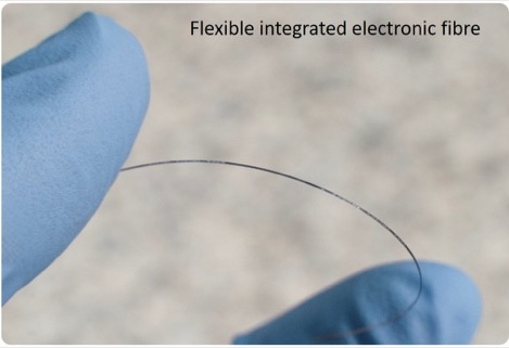
Integrated circuits patterned along a microfibre Flexible integrated electronic fibre held between gloved fingers
System-on-fiber
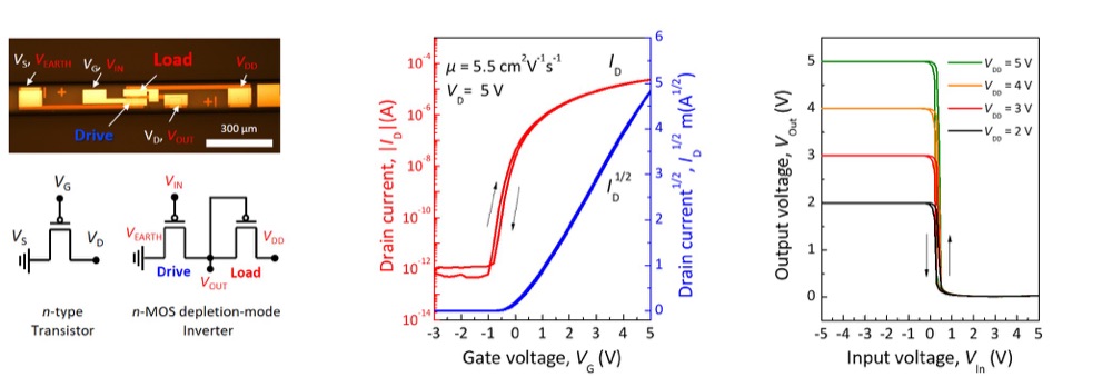
Fiber transistor and inverter architecture
Transistor / inverter
Fiber ring oscillator and electrical characteristics
Fiber logic circuit

A one-dimensional structure becomes a substrate, an interconnect, and a complete electronic system.

  • Chip-on-fiberTransistors, inverters, oscillators, sensors, and interconnects on a single fiber
  • Dual-surface 1DFunctional separation across inner and outer surfaces of hollow architectures
  • Energy fibersHigh-performance harvesting and self-powered sensing in fiber form
  • Distributed textilesWashable computing and sensing networks woven into everyday fabrics
Foundation → frontierChip-on-fiber · Intelligent 1D systems · Self-powered e-textiles

DGIST research vision · 2026 →

From material
to energy system.

Four connected phases move from fundamental discovery to scalable manufacturing and finally to autonomous, multifunctional energy platforms. Each phase creates tools and materials for the next.

Phase 01

Metallene discovery

Advance single-crystalline 2D metals toward a sub-5 nm metallene library through facet engineering and AI-integrated digital discovery.

Atomic-scale precision
Phase 02

Scalable manufacturing

Connect flow chemistry, omni-directional assembly, and roll-to-roll coating to produce uniform films and free-standing active foils.

Lab → continuous process
Phase 03

Emerging 1D Electronics

Combine metallene interconnects, chip-on-fiber integration, and dual-surface 1D architectures for sensing, computing, and energy control.

Fiber → intelligent system
Phase 04

Smart Energy Skin

Converge energy harvesting, radiative cooling, low-voltage heating, and EMI shielding in one adaptive multifunctional film.

Functions → autonomous skin

A forward-looking research direction at DGIST; specific implementations will evolve with scientific findings and collaborations.

Selected research foundation
Evidence for the next chapter.

View all publications →
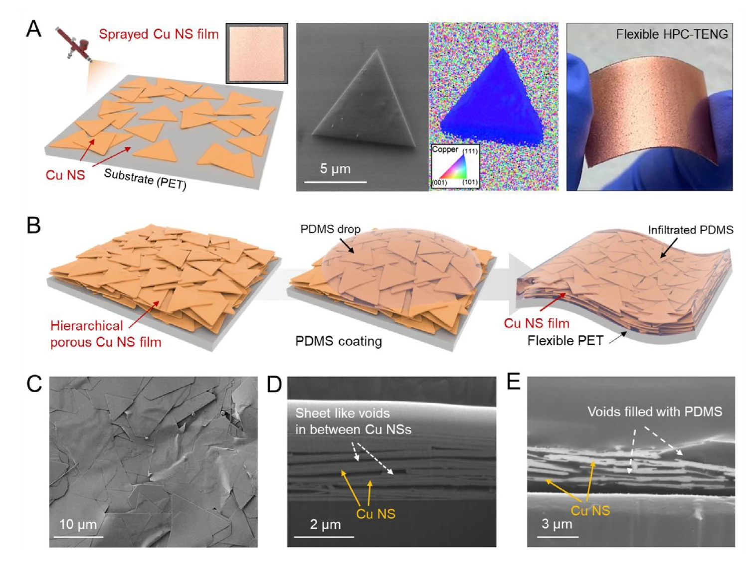
Fabrication and structure of a hierarchical porous copper nanosheet film
FIG. 01Hierarchical porous Cu nanosheet architecture
Advanced Materials · 2025590%

Hierarchical porous 2D metal nanosheet TENG

Output enhancement with more than 100,000 stable cycles, plus EMI shielding and low-voltage heating.
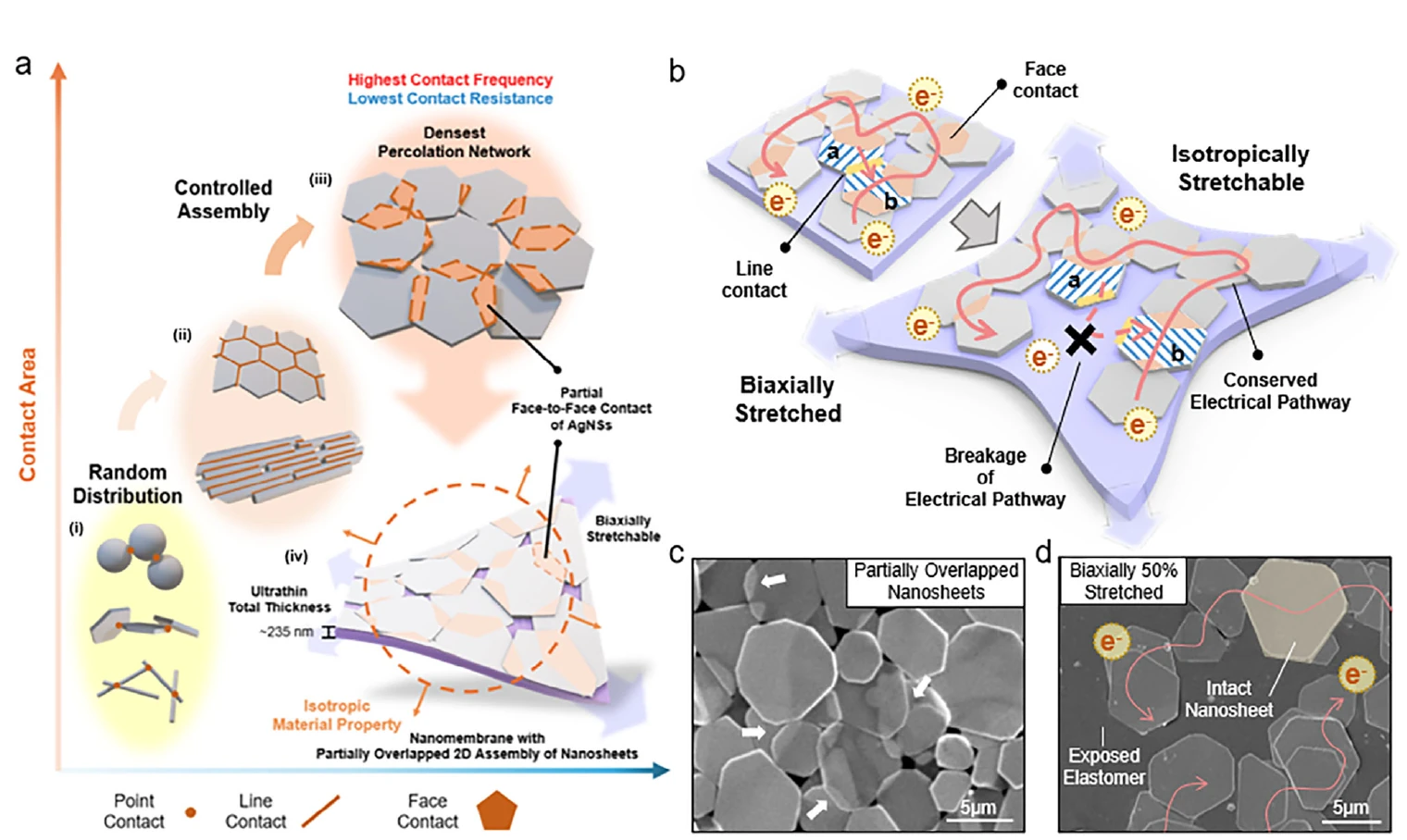
Controlled partial-overlap assembly of silver nanosheets for an isotropic stretchable conductor
FIG. 02Isotropic Ag nanosheet nanomembrane
Advanced Materials · 2025≈115,000

Isotropic Ag nanosheet nanomembrane

S cm−1 conductivity with ≈50% stretchability for tactile electronic skin.
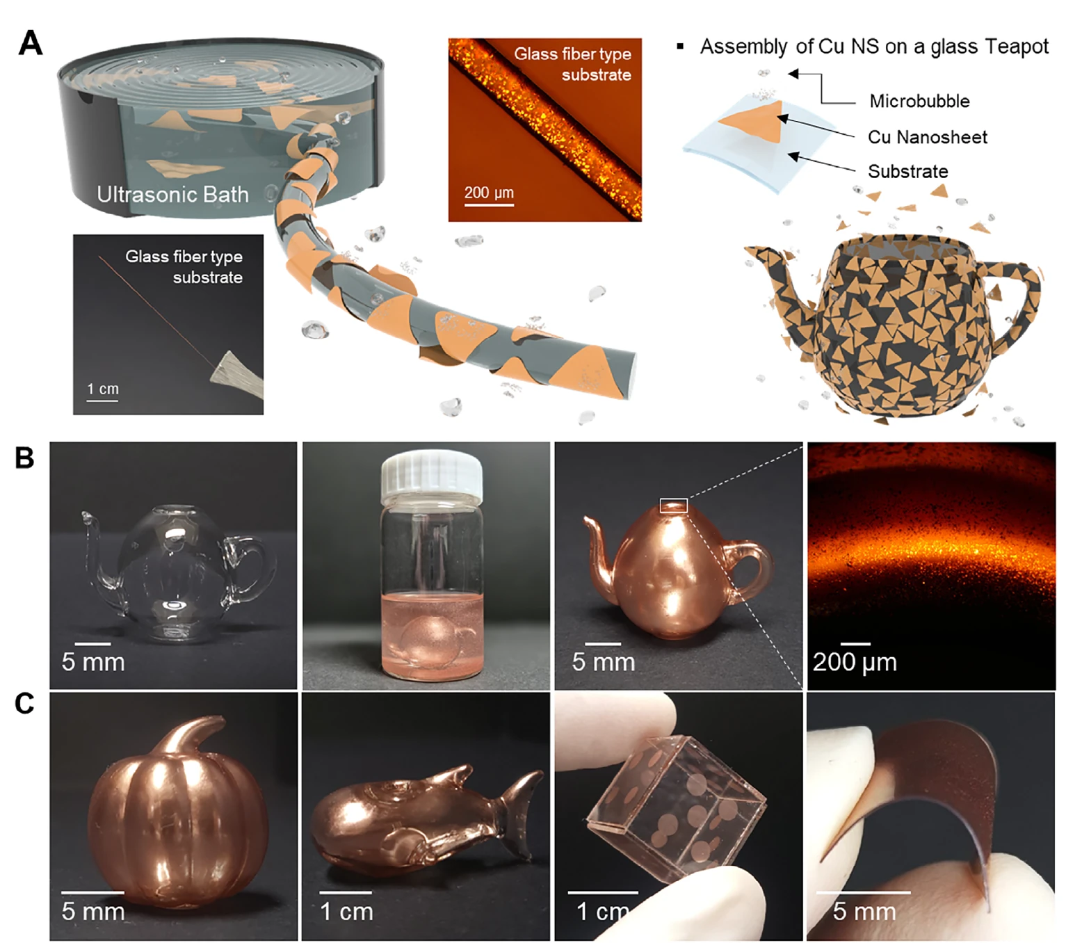
Ultrasonic omni-directional assembly of copper nanosheets on complex objects
FIG. 03Omni-directional assembly on complex surfaces
Advanced Materials · 2025OMNI

Omni-directional nanosheet assembly

Ultrasonic, selective integration of conductive films on planar, curved, flexible, and complex substrates.

Structural and electrical comparison of IGZO transistors with and without single-crystalline silver nanosheets
FIG. 04Ag nanosheet interface in oxide TFTs
ACS Nano · 2025390+

Threshold-engineered oxide transistors

Days of ambient retention using single-crystalline Ag nanosheets at the semiconductor interface.
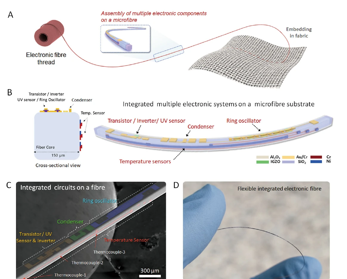
Multiple electronic components integrated along a flexible microfibre
FIG. 05Integrated electronic microfibre platform
Nature Communications · 2022150 μm

Multiple devices on a single microfibre

Transistors, logic circuits, thermocouples, and sensors integrated on a one-dimensional platform and embedded into fabric.

How we work

Make.
Measure.
Understand.
Integrate.

  1. 01
    Synthesize

    Control dimensionality, composition, and crystal structure.

  2. 02
    Assemble

    Build interfaces and architectures across length scales.

  3. 03
    Probe

    Connect materials structure to electrical and electrochemical behavior.

  4. 04
    Integrate

    Translate function into circuits, fibers, and energy systems.

연구의 즐거움

PLAY
RESEARCH.

Curiosity is not separate from rigor. We explore boldly, test precisely, and build together.

Join APPND Lab