
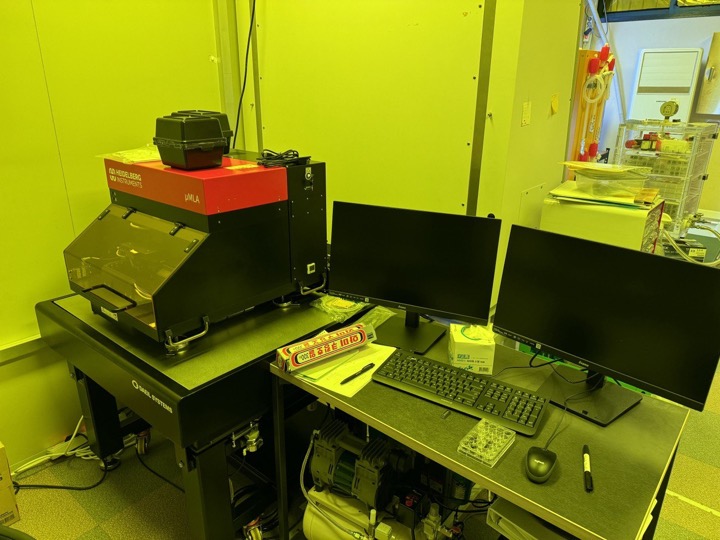
Maskless lithography
Photomask-free micro-patterning for rapid device prototyping
Make · measure · understand
APPND’s experimental workflow connects nanomaterial synthesis and post-processing with thin-film device fabrication, electrical characterization, and electrochemical analysis.
Photomask-free micro-patterning for rapid device prototyping
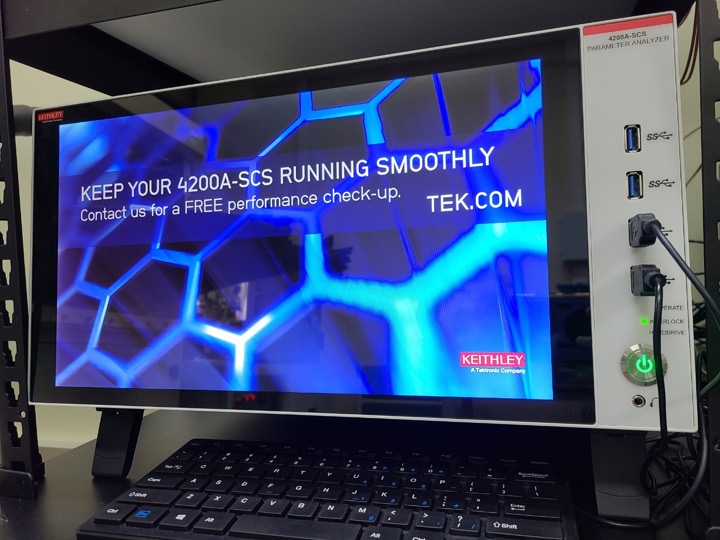
Keithley 4200SCS · HP4145B
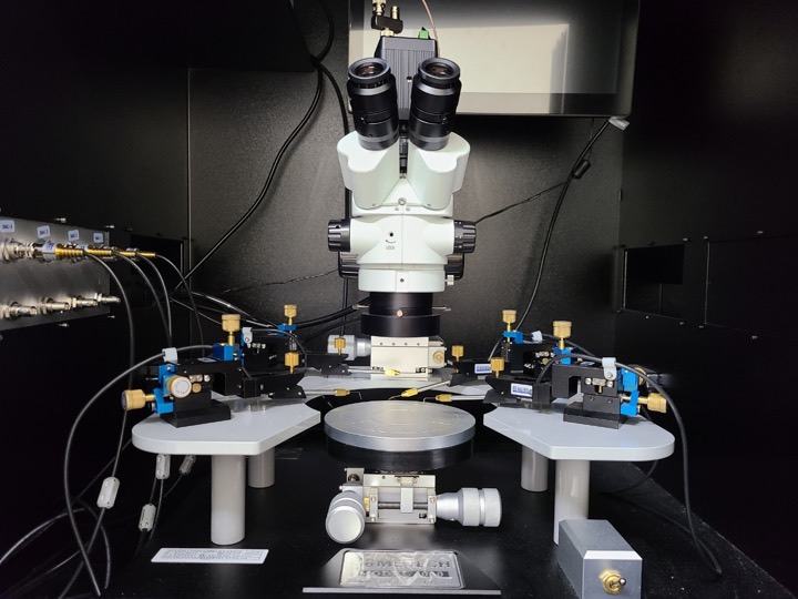
Current–voltage measurement of transistors, memories, and sensors
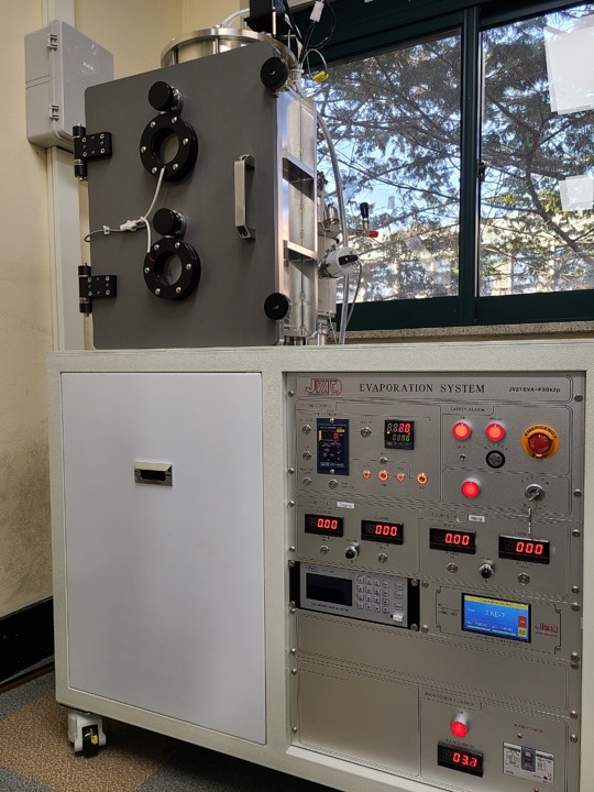
Metal and electrode deposition for device fabrication
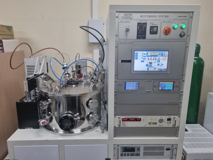
Metal and dielectric thin-film processing
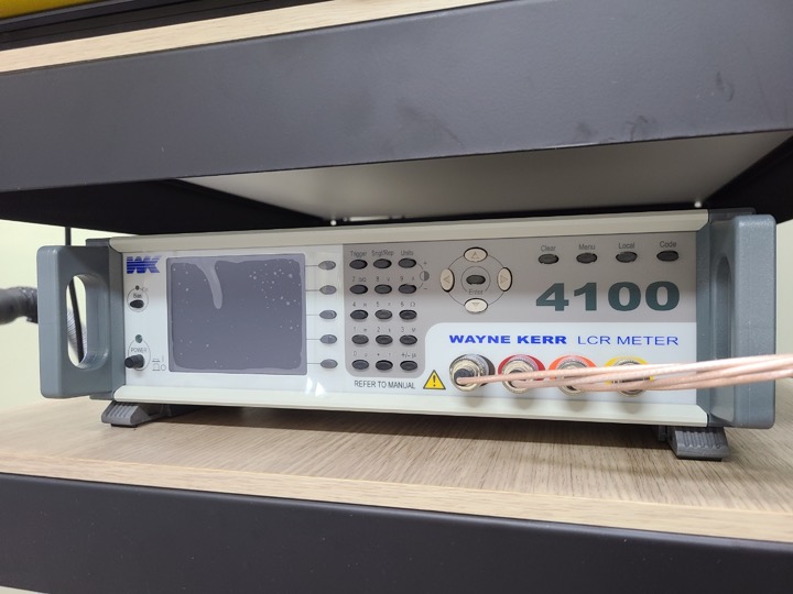
Capacitance, impedance, and frequency-response analysis
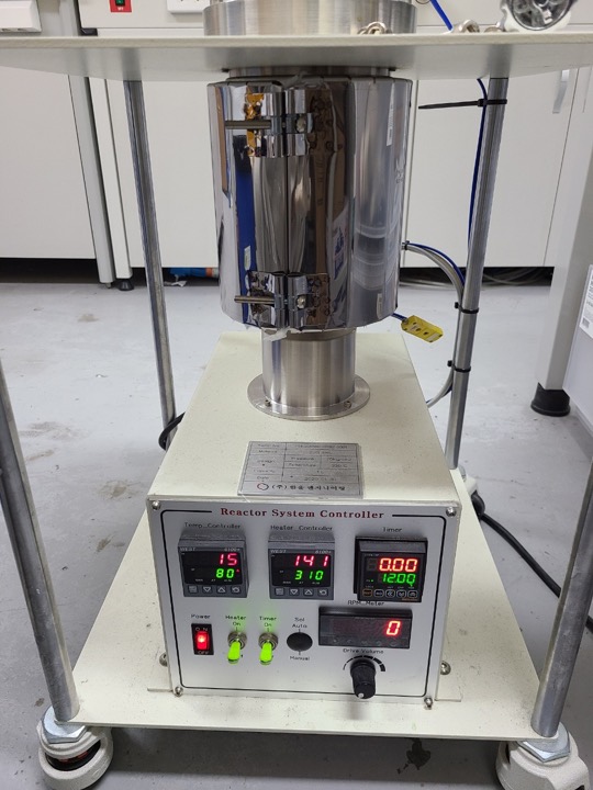
Hydrothermal synthesis of metal and semiconductor nanostructures
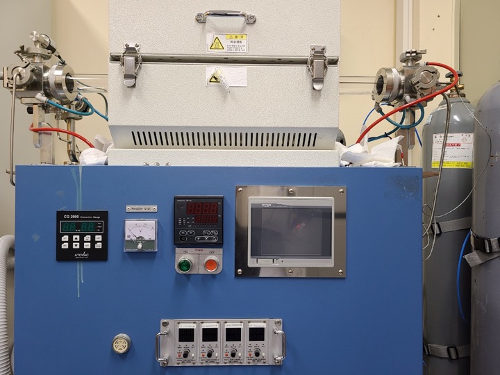
Thermal treatment and vapor-phase material growth
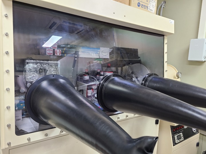
Air-sensitive material synthesis and device handling
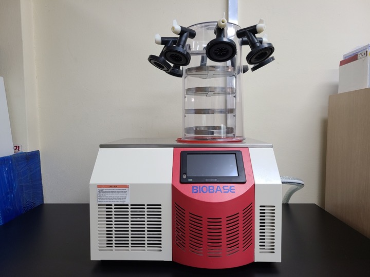
Low-damage drying for porous and high-surface-area structures
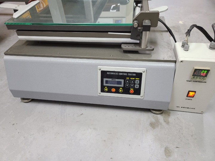
Uniform thin-film and large-area coating from inks
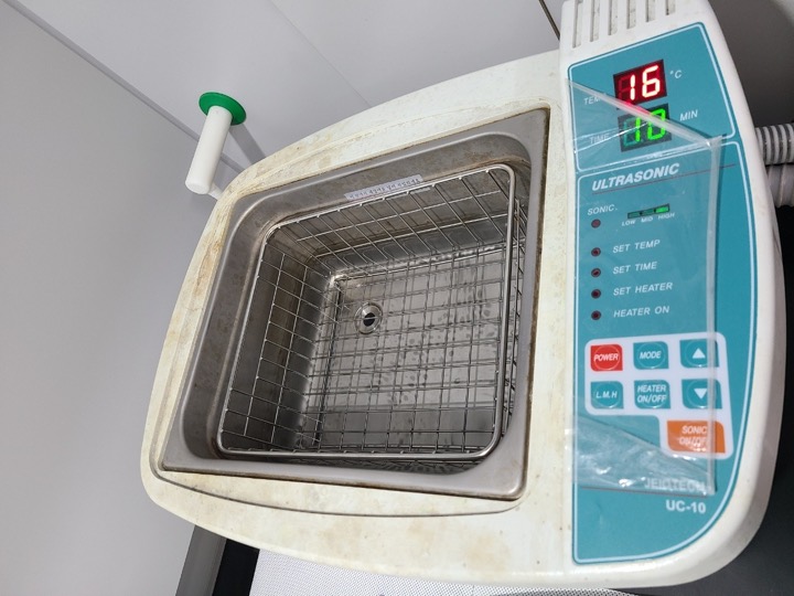
Nanoparticle dispersion, mixing, and exfoliation
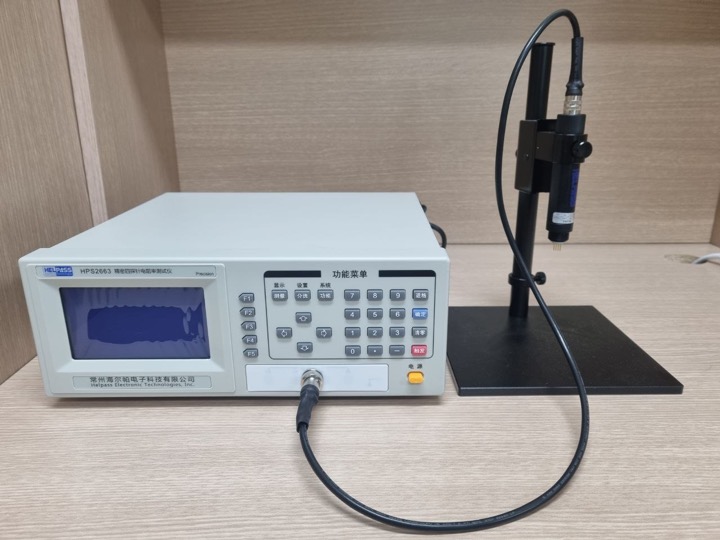
Four-terminal sheet-resistance measurement of conductive films
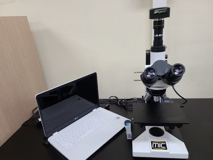
Surface, pattern, and device inspection
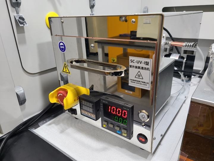
Organic-residue removal and surface-energy control
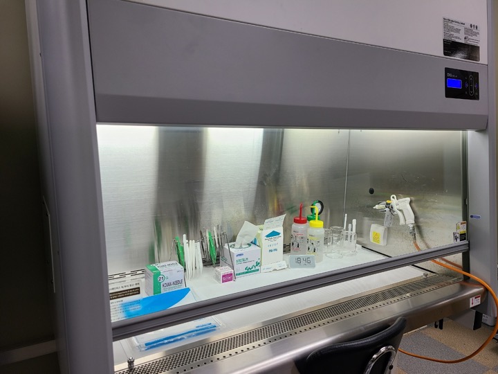
Particle-reduced sample preparation and device assembly
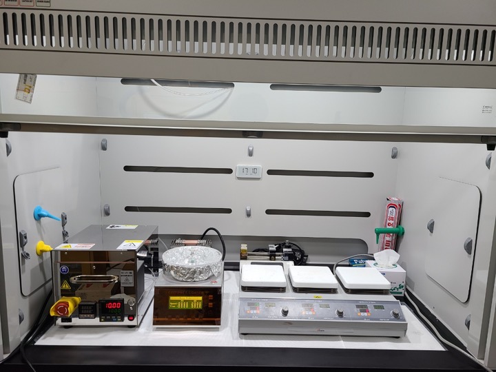
Safe wet-chemical synthesis and sample processing
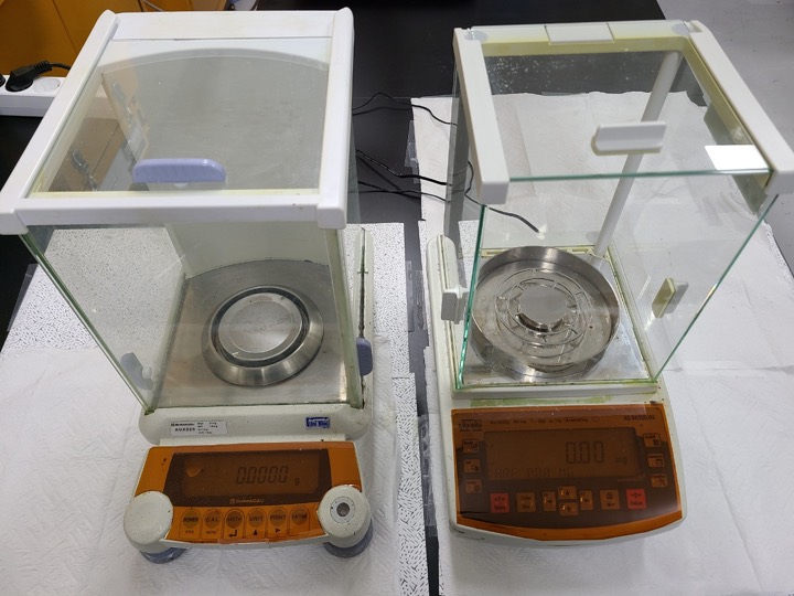
Mass measurement for formulations and electrochemical samples
Equipment access: capabilities may combine APPND-owned instruments with DGIST shared facilities. Contact the laboratory in advance to confirm availability, training requirements, and sample compatibility.